
 关注
关注
已关注
![]() 已认证
已认证
粉丝量 0


核心参数
仪器种类: 电化学工作站
产地类别: 进口
电流范围: -
电流精度: -
电位精度: -
恒电位范围: -
交流阻抗频率范围: -
热门推荐

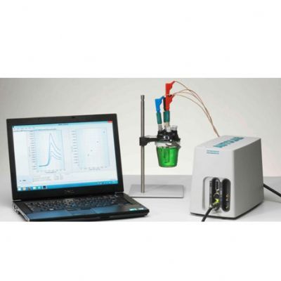
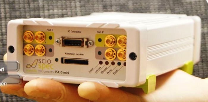
Sciospec ISX-3mini – Electrical Impedance Spectroscopy
Measurement Parameters
![]()
impedance | absolute value of impedance, phase of impedance in degree, phase of |
impedance in radiant, resistance, reactance, absolute value of | |
admittance, phase of admittance in degree, phase of admittance in | |
radiant, conductance, susceptance | |
Measurement Terminal | |
configuration | Two times four wire configuration, three wire configuration, two wire |
configuration (counter C, reference R, work W, working Sense WS) | |
connector type | two times four MCX (female, standard polarity) connectors, |
Sciospec ExtensionPort | |
Sciospec ExtensionPort | |
connector type | Samtec FCS8 20 Pin |
signal level standard | LVCMOS 3V |
maximum input voltagei | 3.6V |
minimum input voltage | -0.3V |
high level input voltage | ≥1.7V |
low level input voltage | 0.8V |
high level output voltage | ≥2.8V |
maximum output current | 12mA |
ESD protection of IOs | ±12kV IEC 61000-4-2 contact ESD |
±15kV IEC 61000-4-2 air-gap ESD | |
clamp voltage 10.5V (min) | |
break-down voltage 7V (min) | |
number of IOs | eight total (freely distributable between input and output) |
IO configuration | GPIO, UART, I2C |
measurement terminals | four (counter C, reference R, work W, working sense WS) |
power terminals | ±5V; 500mA for each voltage |
pin assignment | see Tab 1, shielding GND |
connector Layout | see Fig 1 |
![]()
![]()
![]()
Data she e t Sci o spe c I SX - 3m i ni
J une 20 14
![]()
PIN | ||||||||||||||||||||
1 | 2 | 3 | 4 | 5 | 6 | 7 | 8 | 9 | 10 | 11 | 12 | 13 | 14 | 15 | 16 | 17 | 18 | 19 | 20 | |
Mode | ||||||||||||||||||||
GPIO | W | +5V | +5V | +5V | +5V | WS | IO1 | IO2 | IO3 | IO4 | IO5 | IO6 | IO7 | IO8 | R | -5V | -5V | -5V | -5V | C |
I2C | W | +5V | +5V | +5V | +5V | WS | SCK1 SDA1 | SCK2 | SDA2 | d.n.c. | d.n.c. | d.n.c. | d.n.c. | R | -5V | -5V | -5V | -5V | C | |
UART | W | +5V | +5V | +5V | +5V | WS | Rx | Tx | d.n.c. | d.n.c. | d.n.c. | d.n.c. | d.n.c. | d.n.c. | R | -5V | -5V | -5V | -5V | C |
Tab 1: ExtensionPort pin assignment for differnet modes of operation (d.n.c. ... do not connect)

Fig 1: ExtensionPort Pin Assignment
Frequency
range | 100mHz to 10MHz | |
resolution | 10mHz (depending on frequency range setting) | |
precision absolute | ±100ppm (at 25°C) | |
temperature drift | ±10ppm over operating temperature range | |
long time stability | ±5ppm first year | |
Voltage Signal | ||
range | 1mV to 1000mV peak-amplitude | |
resolution | 0.1 mV | |
Output Impedance | ||
output impedance | 300? (nominal) | |
DC Bias | ||
voltage range | 0V to 8V (see Fig 7) | |
voltage resolution | 10 mV | |
current range | 0A to 20mA (see Fig 7) | |
current resolution | 25μA | |
Precision settings | ||
precision range | 0 to 1 high speed, lower accuracy | |
1 | standard configuration |Z|/|Z|<0.1% | |
1 to 10 high accuracy, low speed | ||
see Fig 5 and Fig 6 | ||
averaging | 1 to 1024 | |
![]()
![]()
![]()
![]()
![]()
![]()
![]()
Data she e t Sci o spe c I SX - 3m i ni
J une 20 14
Sweep Settings
![]()
available sweep | frequency, amplitude, DC bias voltage, DC bias current, kinetic, |
parameters | point delay |
sweep type | linear, logarithmic, list |
points | 1 to 2048 |
sweep delayii | 0s to 3min in 1μs steps |
point delayiii | 0s to 3min in 1μs steps |
Synchronisation Ports (SyncPort) | |
sync ports | two inputs, two outputs, |
sync input type | point hold off, sweep hold off, immediate stop |
sync output type | sweep complete, point complete |
connectors | four SMA (female, standard polarity) |
ESD protection | ±12kV IEC 61000-4-2 contact ESD |
±15kV IEC 61000-4-2 air-gap ESD | |
clamp voltage 10.5V (min) | |
break-down voltage 7V (min) | |
absolute maximum input | 5.5V |
voltage i | |
absolute minimum input | -0.3V |
voltage | |
high level input voltage | ≥2V |
low level input voltage | ≤0.8V |
high level output voltage | ≥2.7V (open drain buffer with 1kOhm pull up resistor to 3V) |
low level output voltage | ≤0.55V |
maximum output current | 24mA |
typical input capacitance | 3pF |
IO Port | |
connector type | D-Sub-Mikro-D 20Pin |
signal level standard | LVCMOS 3V |
absolute maximum input | 3.6V |
voltage i | |
absolute minimum input | -0.3V |
voltage | |
high level input voltage | ≥1.7V |
low level input voltage | ≤0.8V |
high level output voltage | ≥2.8V |
low level output voltage | ≤0.2V |
maximum output current | 12mA |
ESD Protection of IOs | ±12kV IEC 61000-4-2 contact ESD |
±15kV IEC 61000-4-2 air-gap ESD | |
clamp voltage 10.5V (min) | |
break-down voltage 7V (min) | |
number of IOs | eight (freely distributable between input and output) |
![]()
![]()
![]()
Data she e t Sci o spe c I SX - 3m i ni
J une 20 14
IO configuration | GPIO, UART, I2C | ||||||||||||||||||||||||
UART configuration | 115.2kBaud, 1 start bit, 8 data bits, 1 stop bit, even polarity, idle high | ||||||||||||||||||||||||
I2C configuration | 100kbit, 7bit address, standard mode, device behaves as master | ||||||||||||||||||||||||
number of | 2 | ||||||||||||||||||||||||
temperature sensors | |||||||||||||||||||||||||
temperature sensor type | Negative temperature coefficient (NTC) | ||||||||||||||||||||||||
configurable: Reference resistance, reference temperature, Beta value | |||||||||||||||||||||||||
pin assignment | See Tab 2 | ||||||||||||||||||||||||
connector layout | See Fig 2 | ||||||||||||||||||||||||
PIN | 1 | 2 | 3 | 4 | 5 | 6 | 7 | 8 | 9 | 10 | 11 | 12 | 13 | 14 | 15 | 16 | 17 | 18 | 19 | 20 | |||||
Mode | |||||||||||||||||||||||||
GPIO | GND | NTC1 | GND | NTC2 | GND | IO1 | GND | IO2 | GND | IO3 | GND | IO4 | GND | IO5 | GND | IO6 | GND | IO7 | GND | IO8 | |||||
I2C | GND | NTC1 | GND | NTC2 | GND | SCK1 | GND | SDA1 | GND | SCK2 | GND | SDA2 | GND | d.n.c. | GND | d.n.c. | GND | d.n.c. | GND | d.n.c. | |||||
UART | GND | NTC1 | GND | NTC2 | GND | Rx | GND | Tx | GND | d.n.c. | GND | d.n.c. | GND | d.n.c. | GND | d.n.c. | GND | d.n.c. | GND | d.n.c. | |||||
![]() Tab 2: IO Port pin assignment for different modes of operation
Tab 2: IO Port pin assignment for different modes of operation

Fig 2: IO Port connector
LAN Interface
standard conformity | 10/100 Base-T, RJ45 |
protocol | TCP/IP |
USB Interface | |
standard conformity | USB 2.0 Type B |
protocol | High Speed USB |
General Specifications | |
power requirements | 12VDC (typ.), 15W (max), Connector DC Jack (Type: Switchcraft 712A) |
dimensions | 184.0mm x 54.8mmx 113.1mm (width x height x depth) |
see Fig 3 and Fig 4 | |
weight | 1.0kg (typical) |
operating conditions | 0°C to 40°C, <80% relative humidity non condensing, 0...3000m altitude |
non-operating conditions | -25°C to 80°C, <80% relative humidity non condensing1 |
![]()
![]()
![]()
1 The temperature gradient should not exceed 1K/min to reach operating conditions.

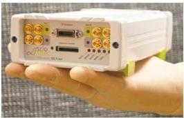
Fig 3: ISX-3mini front view

Specifications
All specifications above are stated for operation at temperatures between 0°C and 40°C. Warm-up time must be greater than or equal to 30 minutes after power on for all specifications.
Electro static discharge Warning
![]()
This product, like all electronic products, uses semiconductors that can be damaged by electrostatic discharge (ESD). When handling, care must be taken so that the devices are not damaged. Damage due to inappropriate handling is not covered by the warranty.
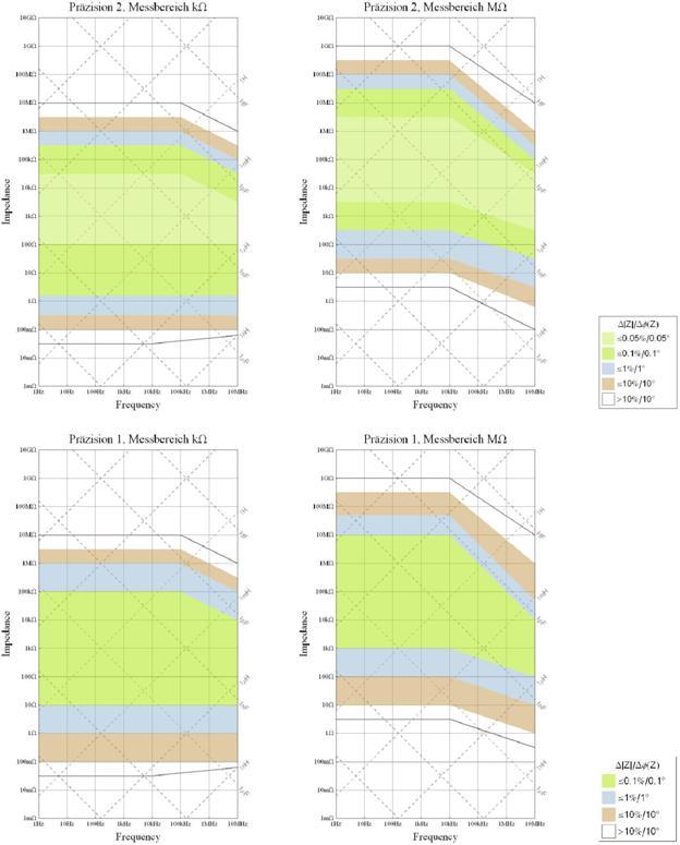
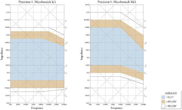
Relation between the precision setting and the measurement time and measurement accuracy


Overview of the different range and precision settings


Fig 8: Precision-Range Plot
All specifications refer to measurements done with a Sciospec ISX-3mini in combination with the Sciospec MEArack. The signal amplitude is set to 100mV and the frequency range to ?<10MHz“. Measurements done, using the BNC connectors show very similar results.
Example measurement:
Frequency sweep: 100Hz – 1MHz, 80 logarithmic Frequency steps, precision 1, amplitude 100mV, measurement range MΩ
Measurement instrument: Sciospec ISX-3mini with connected Sciospec MEArack
DUT: Multielectrode array, 40μm electrodes, 200μm apart, platinum PBS buffersolution

i Inputs are internally biased to 3V by a 1MOhm pull up resistor.
ii Sweep-Delay…Timing delay between two consecutive measurements of complete impedance spectra
Point-Delay…Timing delay between two consecutive measurements of single frequencies
企业名称
海蓝嘉胜科技(北京)有限公司
企业信息已认证
企业类型
信用代码
110105014903607
成立日期
2012-05-15
注册资本
500
经营范围
海蓝嘉胜科技(北京) 有限公司
公司地址
朝阳区望京东亚望京中心A座2712室
客服电话
公司名称: 海蓝嘉胜科技(北京) 有限公司
公司地址: 朝阳区望京东亚望京中心A座2712室 联系人: 王女士 邮编: 100102
仪器信息网APP

展位手机站