
 关注
关注
已关注

![]() 已认证
已认证
粉丝量 0
400-860-5168转2623
仪器信息网认证电话,请放心拨打
两相流,多相流层析成像仪器样本
2014-02-14 14:22
浏览:277次
分享:资料摘要:
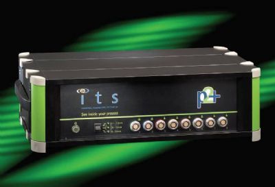
供应ITS P2+电阻层析成像仪器
型号: P2+
产地:
品牌:
面议
参考报价
下载本篇资料:
下一篇
M3C电容层析成像仪器
相关资料
DynaFlex 是汽车白车身在线检测系统:主要针对汽车白车身的孔,插槽,螺钉,螺母,边缘,轮廓,表面点,表面平整度等在线检测,系统可以在40秒内完成对整车的全检。检测每个点只需要3秒钟。另外:我们系统也可以检测汽车零部件,例如:车门、车架、引擎盖等。
The Kelvin Probe method is a relative one. To determine the absolute work function of the sample the vibrating tip has to be calibrated against another “reference” surface. However the value of the tip work function is obviously only as good as the value taken for the reference surface. As a reference sample an aluminum metal plate covered with a thin gold layer has been used (fig. 2). Based on our experiments we assume the gold reference work function as 5.10 eV. The objective of this sample is to measure the contact potential difference (CPD) on the gold surface, and taking the gold reference as 5.10 eV to calculate the tip work function
The scanned sample have been mounted on a aluminum sample holder (fig. 3). Before each SPV measurement the smples have been stored in dark for 12 hours. The contact potential difference (CPD) measured after the 12 hours has been taken as the zero level. The results presented in section 2 show an absolute surface potential change due to light illumination. All measurements have been made in ambient at a temperature of 20±2°C and relative hum idity of 41 ± 2%. In section 3 we presented the light source characteristics
We have applied a high resolution scanning Kelvin probe to perform dark surface potential topographies of multicrystalline silicon solar cells having thin coatings of Si3N4 and SiO2. We clearly observe the electrical characteristics of the screen printed bus-bar and associated fingers, grain boundaries, together with characteristic structures on the oxide and nitride, coupled to significant surface potential variations across larger sections of the wafer. Associated surface photovoltage measurements can be unambiguously decoded to show coating and bulk contributions. The nitride coating exhibits carrier trapping lifetimes in excess of 13 minutes at 300K.
公司名称: 上海沃埃得贸易有限公司
公司地址: 上海市闸北区共和新路3699号共和国际A1707 联系人: 朱云国 邮编: 200032 联系电话: 400-860-5168转2623
仪器信息网APP

展位手机站