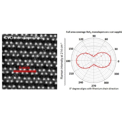
This product contains full area coverage ReS2 monolayers on c-cut sapphire substrates. Sample size measures 1cm in size and the entire sample surface contains monolayer thick ReS2 sheet. Synthesized full area coverage monolayer ReS2 is highly crystalline, some regions also display significant crystalline anisotropy.
Sample Properties.
Sample size | 1cm x 1cm square shaped |
Substrate type | Sapphire c-cut (0001) |
Coverage | Full monolayer coverage |
Electrical properties | 1.6 eV Anisotropic Semiconductor (Indirect Bandgap) |
Crystal structure | Distorted Tetragonal Phase (1T’) |
Unit cell parameters | a = 0.630, b = 0.638 nm, c = 0.643 nm α = 106.74°, β = 119.03°, γ = 89.97° |
Production method | Atmospheric Pressure Chemical Vapor Deposition (APCVD) |
Characterization methods | Raman, angle resolved Raman spectroscopy, photoluminescence, absorption spectroscopy TEM, EDS |
Specifications
1) Identification. Full coverage 100% monolayer ReS2 uniformly covered across c-cut sapphire.
2) Physical dimensions. One centimeter in size. Larger sizes up to 2-inch wafer-scale available upon requests.
3) Smoothness. Atomically smooth surface with roughness < 0.2 nm.
4) Uniformity. Highly uniform surface morphology. ReS2 monolayers uniformly cover across the sample.
5) Purity. 99.9995% purity as determined by nano-SIMS measurements
6) Reliability. Repeatable Raman and photoluminescence response
7) Crystallinity. High crystalline quality, Raman response, and photoluminescence emission comparable to single crystalline monolayer flakes.
8) Substrate. c-cut Sapphire but our research and development team can transfer ReS2 monolayers onto variety of substrates including PET, quartz, and SiO2/Si without significant compromisation of material quality.
9) Defect profile. ReS2 monolayers do not contain intentional dopants or defects. However, our technical staff can produce defected ReS2 using α-bombardment technique.
Supporting datasets [for 100% Full area ReS2 monolayers on c-cut Sapphire]
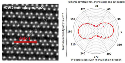
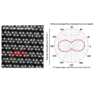
Transmission electron images (TEM) and angle resolved Raman spectroscopy measurements acquired from CVD grown full area coverage ReS2 monolayers on c-cut sapphire confirming crystalline anisotropy.
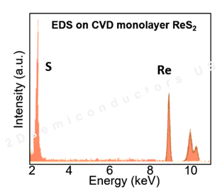
Energy dispersive X-ray spectroscopy (EDX) characterization on CVD grown full area coverage monolayer ReS2 on c-cut sapphire
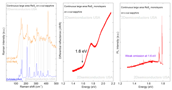
Raman spectroscopy measurement confirm monolayer nature of the CVD grown samples. Differential reflectance measurements clearly show band gap at 1.6 eV for ReS2 consistent with the existing literature values. PL spectrum only display weak emission at 1.6 eV but significantly stronger at lower temperatures.
基于蓝宝石衬底的全区域覆盖的单层二硫化铼信息由上海巨纳科技有限公司为您提供,如您想了解更多关于基于蓝宝石衬底的全区域覆盖的单层二硫化铼报价、型号、参数等信息,欢迎来电或留言咨询。
除供应基于蓝宝石衬底的全区域覆盖的单层二硫化铼外,上海巨纳科技有限公司还可为您提供碲化铋(Bi2Te3)、Telluride 碲化物、基于塑料衬底的石墨烯等产品,公司有专业的客户服务团队,是您值得信赖的合作伙伴。