资料下载:Download Components for DUV-photolithography Datasheet (PDF, 388 KB)
One of the essential requirements of modern optoelectronics consists in miniaturization of equipment and devices as well as the components they include. It dictates the necessity of utilization of DUV lasers as the key tools of advanced photolithographic technology. This type of lasers have shortest (among others laser sources) wavelength of powerful monochromatic radiation. It allows generating nano-scale structures and thus creating systems characterized by the maximal spatial resolution as well as by packing density.
Modern projection steppers and scanners on the base of KrF excimer lasers (248 nm) are currently used to produce lines in the 110 nm range. Lines as thin as 65 nm are being resolved by systems utilizing ArF excimer lasers emitting light with a wavelength of 193 nm. Further resolution enhancement and improvement of the systems became possible using immersion lithography. In this case laser radiation is focused not on dry substrate but on the one moistened by special immersion liquid. This liquid is typically ultra-pure, deionized water continually circulated to eliminate thermally-induced distortions. Such approach has allowed increasing the numerical aperture by more than 30% and as a result it enables the economical volume production of microchips featuring 45 nm structures.
Utilization of synthetic crystal quartz for the purposes DUV-photolithography is caused by its excellent transmission in UV range, high crystallographic perfection and optical homogeneity, chemical resistance and stability to intensive laser radiation.
For production of optical components described in this chapter Tydex uses synthetic crystal quartz of precision optical grade (class A1, category “extra”).
Main parameters of the used material are as follow:
| Parameter | Value |
| Twinnings, striaes, microbubbles including their conglomerates; inclusions and cracks | not allowed |
| Polarization uniformity | no visible variations during inspection between crossed polarizers |
| Homogeneity of refractive index | Δ n < 3 x 10⁻⁶ (TWD <= λ /10 per inch of crystal length) |
| Etch channels, cm-2 | <= 30, typically |
| Absorption coefficient, cm-1 (λ=193 nm) | <= 0.025 |
| Birefringence, nm/cm | <= 10 |
| Concentration of main impurities, ppm | <= 10 |
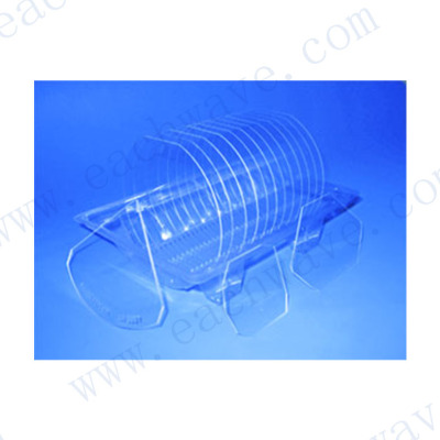
circular plano-plano thin plates (wafers);For DUV-photolithography Tydex supplies the following components:High level of growth technology which is currently used to produce synthetic crystal quartz does ensure that these parameters will be obtained. But high-involved responsibility induced by application dictates a mandatory requirement to check material quality additionally. Moreover any small piece of used material must be tested without exceptions and with double attention to any details. For this purpose prior to passing an ingot to production we cut and prepare a sample of required overall dimensions and then get it polished. After that we accurately test it under UV excitation using ArF excimer laser. Each ingot (i.e. the sample) even being grown at the same growth run must pass this test successfully. A dose and duration of the excitation simulate the further working conditions of finished optical components and are specially selected to make an attempt to discover material imperfections, mainly the impurities. Only the material withstanding the applied exposure and that is the most important thing – do not get UV-induced degradation of transmission, is passed to production. Otherwise or in case if any single parameter does not meet the above mentioned value, the material is unambiguously rejected and it is ensured that it will be never used for the purposes of discussed application.
sector-shape plano-plano plates (sectors);
wedge plates of complex design (depolarizers).
Severe application' conditions where the components are used dictate the exclusive requirements to parameters of their treatment. Typical specification is as follows:
| Parameter | Value |
| Orientation tolerance, arc. min. | +/- 10 |
| Surface quality, scr/dig | High-quality polishing, better than 20/10 |
| Surface roughness at any square of 350 μm x 260 μm (RMS), nm | < 0.6 |
| TWD ( λ= 633 nm), λ | < 1 |
| Thickness of an element, mm: - wafer - sector - depolarizer (thin edge) | 0.55575 1.9456 0.9 |
| Tolerance zone for overall dimensions (excluding thickness), mm | +/-0.05 |
| Tolerance zone for thickness (typical value), μm | +0.5/-2 (+/-0.5 – state-of-the-art) |
| Non-parallelism of opposite surfaces (for plano-plano elements), arc. sec. | < 2 |
| Tolerance zone for wedge (for wedged elements), arc. min. | +/- 25 |
The examples of ZYGO interferograms (TWD) are shown at figures 1-3.Together with each component we supply a certificate of conformance as well as an individual interferometer graph demonstrating surface errors.
 of D100 mm wafer")
Fig. 1 Typical ZYGO interferograms (TWD) of D100 mm wafer.
 of sector")
Fig. 2 Typical ZYGO interferograms (TWD) of sector.
 of depolarizer")
Fig. 3 Typical ZYGO interferograms (TWD) of depolarizer.
Besides the components mentioned above and upon your specification & design we will be glad to produce other custom-made components.
用于深紫外成像的元件 Components for DUV-photolithography信息由上海屹持光电技术有限公司为您提供,如您想了解更多关于用于深紫外成像的元件 Components for DUV-photolithography报价、型号、参数等信息,欢迎来电或留言咨询。
除供应用于深紫外成像的元件 Components for DUV-photolithography外,上海屹持光电技术有限公司还可为您提供波导型PPLN、 光纤跳线、THz 波片,可调谐太赫兹波片等产品,公司有专业的客户服务团队,是您值得信赖的合作伙伴。