
 关注
关注
已关注
![]() 已认证
已认证
粉丝量 0
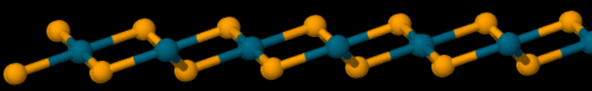
Bulk PdSe2 (palladium diselenide) has been predicted to exhivit 30 meV band gap which increases to 1.43 eV indirect gap (theoretical). In comparison to other TMDCs, PdSe2 has an uncommon structure: Pd atoms coordinate with four Se atoms, forming a square backbone lattice. It has also been recently shown that PdSe2 monolayer immediately undergo PdSe2 to Pd2Se3 crystal transformation. Owing to vast amount of Pd atoms, PdSe2 has been theoretically and experimentally shown to be catalytically active material thoigh fundamental research still remains at its seminal stages.
Growth method matters> Flux zone or CVT growth method? Contamination of halides and point defects in layered crystals are well known cause for their reduced electronic mobility, poor e-h recombination, low-PL emission, and lower optical absorption. Flux zone technique is a halide free technique used for synthesizing truly semiconductor grade vdW crystals. This method distinguishes itself from chemical vapor transport (CVT) technique in the following regard: CVT is a quick (~2 weeks) growth method but exhibits poor crystalline quality and the defect concentration reaches to 1E11 to 1E12 cm-2 range. In contrast, flux method takes long (~3 months) growth time, but ensures slow crystallization for perfect atomic structuring, and impurity free crystal growth with defect concentration as low as 1E9 - 1E10 cm-2. So if your research needs truly high quality crystals for optoelectronics, scanning tunneling microscopy, spectroscopy, and other projects that rely on defect free crystals, flux zone growth is ideal for you. If you need catalytic materials, the presence of defects typically helps. In such case CVT growth crystals are better suited for catalysis. During check out just state which type of growth process is preferred. Unless otherwise stated, 2Dsemiconductors ships Flux zone defect free crystals as a default choice.
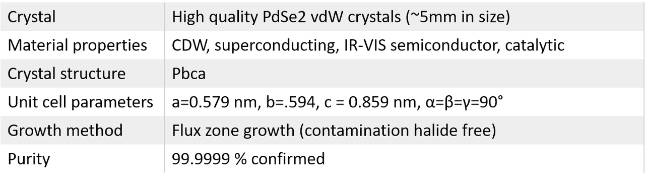
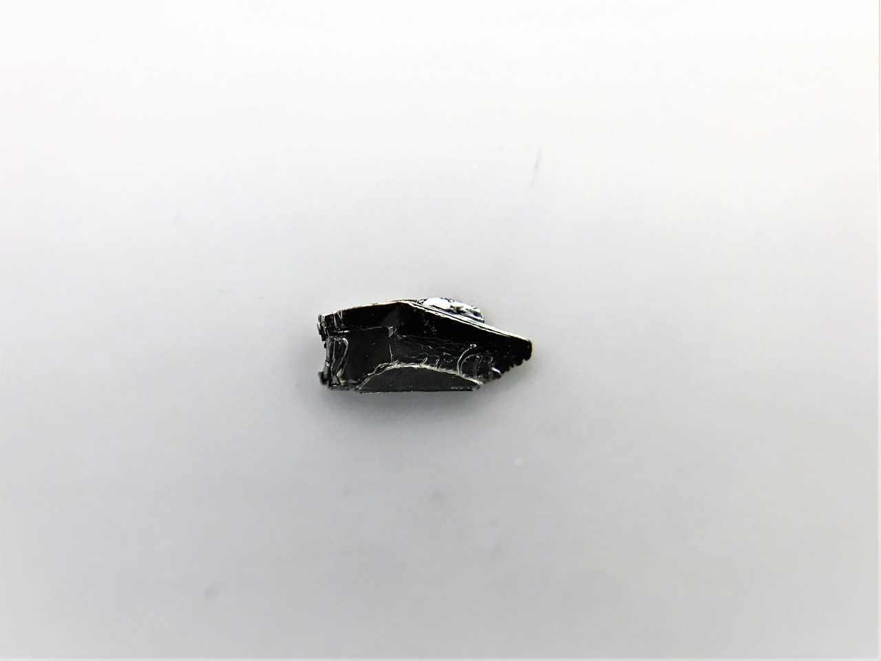
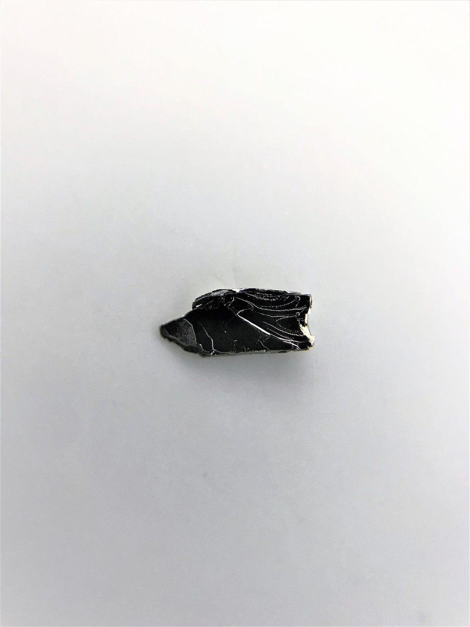
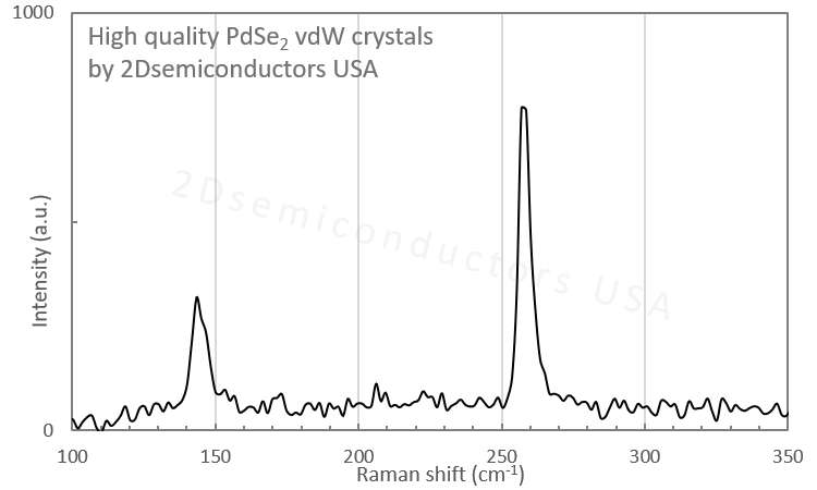
Properties of PdSe2 vdW crystals by 2Dsemiconductors USA

上海巨纳科技有限公司
公司地址
上海市虹口区宝山路778号海伦国际大厦5楼
客服电话
公司名称: 上海巨纳科技有限公司
公司地址: 上海市虹口区宝山路778号海伦国际大厦5楼 联系人: 袁文军 邮编: 200081
仪器信息网APP

展位手机站