
 关注
关注
已关注

![]() 已认证
已认证
粉丝量 0
400-860-5168转0980
仪器信息网认证电话,请放心拨打

核心参数
产地类别: 进口
仪器类型: 立式
温度波动度: 小于10mK(峰-峰值)
工作距离: 水平14.5 mm,竖直9 mm,可集成4 mm或更小近工作距离选件
极限温度: 3.2K-350K (无热负载时低<3K)
震动稳定性: 小于10mK(峰-峰值)
外型尺寸: 桌面式
循环介质: 闭循环制冷,无需消耗液氦
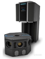
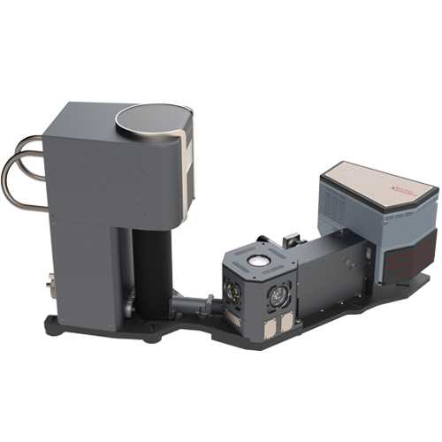
Montana Instruments超精细多功能无液氦低温光学系统
Montana Instruments推出了全新超精细多功能无液氦低温光学系统——CryoAdvanceTM,该系列产品是采用新的性能标准和架构而生产的新一代标准化产品,可使用通用型的光学桌面进行固定,使用方便。采用减震技术和特殊温度稳定技术,在不牺牲任何便捷性的同时,为实验提供的温度稳定性和超低震动环境。如今CryoAdvance系列产品具有多种型号、配置、选件与配件可选,能够满足每个研究人员的特需求。

应用领域
金刚石色心、NV色心、量子计算、量子光学、腔量子电动力学、自旋电子学、磁光克尔效应、单光子发射......
基本特点
★ 低温度波动和纳米的震动可为各种测量提供稳定的实验环境。
★ 超大温区(3.2K - 350K)与超快的变温速度可提高实验效率。
★ 全干式系统,无需消耗氦气或液氦,可大降低实验成本。
实用性优势
★ 直观的用户界面和全自动控制系统提高了实验效率。
★ 电学和光学通道以及样品安装都大地提高了实验灵活性。
★ 完全集成、交钥匙设计方案,让您快速启动和实现研究计划。
★ 桌面式设计方案,方便移动,无缝衔接现有的室温实验方案。
设备介绍

制冷系统
系统采用制冷机闭循环制冷方式,只有少量氦气密封在系统内部,日常运行无需消耗液氦或氦气①
★ 降低成本:日常运行不消耗氦气可在很大程度上降低试验成本。
★ 操作简单:省去了更换氦气瓶和监测氦气量等繁琐的实验工作。
系统采用变频制冷技术,大大的改善了实验的能耗和性能②
★ 低能耗需求:只需单项50Hz 208-240V电力需求,无需水冷机,功率3.6KW。
★ 低噪音:压缩机采用的变频技术在降低能耗的同时较大程度上降低了冷头的工作噪音和震动。
系统架构
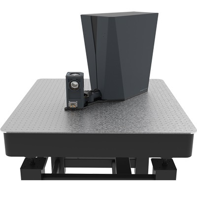
系统采用优化的设计方案,恒温器、样品台可直接固定在任何的光学桌面上③
★ 便捷性:样品腔周围可搭建各种光路,方便实现各种光路实验方案。
★ 灵活性:系统可安装在英制或公制光学桌面,可与螺孔阵列平行或成45°角。
★ 模块化:无需任何额外的辅助设施,可以方便的移动设备。
系统控制
嵌入式程序的触摸屏控制④
★ 全自动、优化的温度控制:简单设定目标温度,一键Cooldown。
★ 其他参数控制:可实现定制化参数控制,例如样品腔除气或干燥氮气冲洗。
★ 监视系统状态:用户界面实时显示系统状态,包括温度、温度稳定性、系统真空度等。
★ 软件记录系统数据:方便数据的导出。
远程控制与其他语言
★ 远程控制:利用虚拟网络计算(VNC)技术,可通过电脑方便地对系统进行远程控制。
★ 外部脚本:支持多种现代语言通过RESTful API脚本控件进行编程控制(Python, MATLAB, LabVIEW, C# 等)。
★ 远程诊断:工程师可以方便的通过网络对设备的故障进行诊断和排除。
系统与真空控制单元的完全自动化流程⑤
★ 完全自动化控制:系统在抽真空、降温、恒温、升温、充气等全过程可以自动设定优化的参数。
★ 完善的系统监控:系统通过自动的过程监控与错误处理保护系统和样品,避免误操作。
★ 干燥氮气清洗选件:抽真空前或充气时可以减少外界大气环境的影响有助于快速降温。
样品环境
样品的安装和更换可直接通过取下外层(真空层)和屏蔽层的盖子即可。
★ 可选择的实验配置:有各种样品安装方案和位置控制选件可供选择,包括光纤和RF探针组件以及用于光子探测的配置。
★ 预置电学接口:系统为用户提供了预置低频电测量和额外温度计安装的直流电学通道。
★ 扩展接口选件:通过侧面板可将RF、光纤、气体和额外的直流通道引入样品腔。
四周和部的窗口方便将各方向的光路引入样品腔。
★ 灵活的光路方案:适应各种测量光路,如透射、侧反射和部显微镜。
★ 超高的收集效率:提供高NA与近工作距离选件。
★ 光学材质:可以轻松更换各种波长和实验需求的窗口。
性能表现
多个和特技术相结合,在不牺牲低温度和制冷功率的基础上优化了热稳定性和震动稳定性。
★ 实现低温度:采用特有的材料和热阻尼技术,使系统在给定的配置下达到尽可能低的温度。
★ 满足震动敏感测量:采用的减震技术,隔冷头震动的同时对样品采用刚性支撑结构,实现纳米的超低震动。
★ 全温区保持样品的光路准确性:采用膨胀系数抵消式结构,保证全温区范围内样品的超低位置漂移。
★ 保证每一个温度点的稳定性:采用主动与被动参数控制技术,使每一个温度点的温度波动减小到传统制冷机波动的二十分之一。
CE认证
系统是非常成熟的定型化产品,已取得CE认证。
设备型号
低温光学
■ CryoAdvanceTM 50低温平台
CA50是新型超精细多功能无液氦低温光学系统的基本型号。该系统具有传统恒温器不可比拟的优势。CA50样品腔具有5个光学窗口,可配置近工作距离选件。该型号是标准低温系统系列中选件兼容性广泛的恒温器,可与多种选件或定制零件进行搭配以满足各种实验需求。

CryoAdvanceTM 50
超震动稳定性:样品台震动的峰-峰值<5nm
优异的温度性能:大的控温范围,3.2K-350K ;温度稳定性佳,在限低温时温度波动始终小于10mK(峰-峰值);超快变温速度,Cool down:~2 小时(如果配置复杂,可能长于2小时)。
光学窗口:5个光学窗口,部1个,侧面4个,特殊窗口可定制。
光路张角:全角60度样品处于样品腔中心位置;全角80度样品处于靠近冷窗位置;全角120度样品处于靠近热窗位置。
工作距离:水平14.5 mm,竖直9 mm,可集成4 mm或更小近工作距离选件。
水平光路高度:140 mm
窗口材料:冷窗与热窗均可镀增透膜,波长范围 400-1000nm,非常方便用户自己更换窗口材料。
电学通道:20条集成直流通道,外加双RF+25DC接口面板。
接口面板:1块可配置面板,可升光纤、高频、气路等。
样品环境:真空、高真空(机械泵、分子泵系统可选)
自动控制:全新智能触摸屏系统,自动升降温、抽真空、充气。
样品移动:可集成三维位移器和二维旋转台
■ CryoAdvanceTM 100低温平台
CA100是CryoAdvanceTM系列低温系统是为满足较为复杂的实验方案而推出的中型样品腔型号。CA100具有较大的样品空间,可满足更多的线路或高频线路接入,可集成横向的镜头,满足横向共聚焦光路的搭建,可集成多组位移器。该型号是标准系列中定制化方案更灵活的型号,可以满足配置较为复杂的低温实验。

CryoAdvanceTM100
模块化的接线面板:在样品腔中提供模块化的低温接线面板,接线模块可满足多种接线类型(交、直流、射频、光纤),大大提升了实验的灵活性。
样品空间:CA100的样品腔尺寸介于CA50和CA200之间,兼顾降温时间和样品腔空间,在尽量小的影响降温速率前提下尽可能的增加了样品空间,使用户可以设计较为复杂的光学实验。
光学灵活性:更大的空间意味着可以容纳更多的光学元件,样品位置也可以有更多的选择。
优异的温度性能:3.4K - 350K; Cool down to 4.2K:~3小时
震动稳定性:<15 nm(峰-峰值)
样品腔空间: Φ100 mm ×116 mm
光学窗口:5个光学窗口,部1个,侧面4个特殊窗口可定制。
光路张角:全角27.5°样品处于样品腔中心位置;全角80°样品处于靠近冷窗位置;全角120°样品处于靠近热窗位置
工作距离:水平28 mm,竖直9 mm;可集成4 mm或更小近工作距离选件
电学通道:25集成式DC通道,4RF接口面板。
接口面板:5个,可升RF,DC,光纤,气路等。
样品移动:可集成位移器,实现三维移动和二维旋转。
■ Cryostation® S200无液氦光学低温恒温器
为了使用户有更大的空间进行复杂低温试验的设计,Montana Instruments研发了大型系统Cryostation® S200。该型号是标准恒温器系列中的大型号。直径196mm的样品腔使用户可以在低温区域搭建复杂的光路。
Cryostation®S200
样品台:低温样品台为带螺孔的标准光学面包板,可以任意设计光路。
光学灵活性:9个光学窗口,支持多根光纤接入。
样品空间:Ф196 mm样品腔可满足各种光学实验需求。
集成式系统
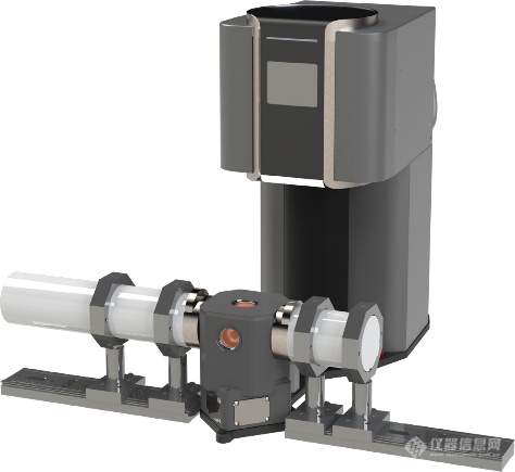
■ CRYO-OPTIC®物镜集成系统
CRYO-OPTIC®系统将光学物镜集成到低温系统的样品腔中,在低温下实现超稳定、高质量的大数值孔径成像。CRYO-OPTIC®系统的设计消除了在低温设备中使用高倍物镜时所面临的对准和漂移问题。
系统对配件和选件具有良好兼容性,允许用户自定义设备的具体配置以满足特的实验需求。可选内置的XYZ纳米位移器用于样品定位和聚焦,可选快速变温样品台,用于样品的快速变温控制。
性能优势
★ 技术允许集成物镜保持在室温,确保超稳定的位置和焦点控制。
★ 对高倍物镜和样品的温度进行主动控制,使其温度稳定性在10 mK 以内,超高的稳定性使其在较小的温度变化后无需重新聚焦。
★ 通过将物镜从恒温器和实验室环境中分离出来,立控制,系统达到稳定测量条件所需的时间大大减少。
■ CryoAdvanceTM50 - CO(竖直物镜集成系统)
该方案是为竖直共焦显微镜设计的,同时系统具有侧面光学窗口,允许用户看到样品和焦距的大致调节。

■ CryoAdvance™100– CO(水平物镜集成系统)
CA100 - CO的水平安装方案可与其他光学测量系统无缝衔接,允许快速、方便的更换样品。特的辐射屏蔽层设计保证更换样品的同时不改变物镜的位置,确保物镜始终处于光路的佳位置。

■ Cryostation S200 – CO(定制物镜集成系统)
Cryostation S200可以实现定制化的物镜集成。物镜水平安装,与低温面包板组成自由光路,可通过压电位移器实现光路的调节。

■ MAGNETO-OPTIC(MO)磁体集成系统
MAGNETO-OPTIC直接将磁体集成到低温样品腔中。这一附加模块不影响系统本身的稳定性,磁体系统具有完全自动化的控制系统。系统可兼容多种选件和配件,包括内置压电位移器等。用户可选择不同配置以满足特的实验需求。
性能优势
★ 设备安装简单,具有特的设计,保证便捷的样品更换和光路便捷性。
★ 自动退磁,采用震荡归零的方式减小电流,以消除磁场设置为零时的剩余磁场。
★ 完备系统,系统包括校准霍尔探头、电源和循环冷却系统,用户无需额外辅助设备。

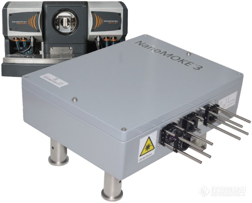
■ CryoMOKE低温磁光克尔集成系统
为了满足用户变温MOKE的测量需求,该系统结合了英国Durham公司的NanoMOKE3系统。该集成系统利用MAGNETO-OPTIC的灵活性与NanoMOKE3的强大功能为用户打造了高性能的低温磁光克尔测量平台。
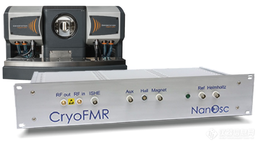
■ CryoFMR低温铁磁共振集成系统
Montana Instruments 为用户提供高精度的低温铁磁共振集成系统。使得样品可以在不同温度、光照情况下进行铁磁共振实验,方便研究样品在光激发状态下的磁学特性。该系统配备NanOsc Instruments AB公司的高精度铁磁共振测试仪,并且操作简单。
■ Cryo Mossbauer低温穆斯堡尔集成系统
Cryo Mossbauer系统提供完整的集成式变温透射穆斯堡尔测量方案。Montana Instruments 采用了MS96光谱仪与Montana恒温器的用户友好型集成方案,设备简单易用。两个领域的全球厂商确保了设备的可靠性。
用户单位
北京大学 | 华中科技大学 |
山西大学 | 山西大学 |
都师大 | 清华大学 |
苏州纳米所 | 中国科学技术大学 |
中国科学技术大学 | 中科院理化所 |
中科院半导体所 | 南京大学 |
中国科学技术大学 | 中国科学技术大学 |
中科院理化所 | 中国科学技术大学 |
南京大学 | 中国科学技术大学 |
上海理工大学 | 南开大学 |
中山大学 | 中国科学技术大学 |
北京大学 | 中科院半导体所 |
中国科学技术大学 | 复旦大学 |
中科院半导体所 | 武汉大学 |
西南交通大学 | 苏州科技学院 |
清华大学 | 中科院半导体所 |
山西大学 | 东南大学 |
中国科学技术大学 | 中国科学院上海高等研究院 |
南开大学 |
部分应用案例
■ 无褶皱超平石墨烯的变温拉曼测量
南京大学高力波教授、奚啸翔教授等多个课题组合作,采用质子辅助的CVD方法生长制备出了无褶皱的超平石墨烯。该方法成功解决了传统CVD制备石墨烯过程中由于石墨烯与基质材料强耦合作用而形成的褶皱,这为石墨烯在二维电子器件等领域的应用扫除了一大障碍。文章表明,在质子辅助的CVD制备方法中,质子能够渗透石墨烯,对石墨烯和衬底之间的范德瓦尔斯相互作用进行去耦合,使褶皱完全消失。该方法还可以对传统CVD制备过程中产生的褶皱进行很大程度的去除。此外,通过新方法制备的超平石墨烯材料,不仅具有优异的清洁能力,还在测量中展示了室温量子霍尔效应。研究认为,质子辅助的CVD方法不仅能制备出高质量的石墨烯,并且对制备其他种类的纳米材料具有普适性,为制备高质量的二维材料提供了一种新途径。相关成果发表在Nature。
值得一提的是,文章中对样品进行了高质量的变温Raman测量(南京大学物理学院奚啸翔教授通过Montana Instruments公司生产的Cryostation®系列高性能恒温器与普林斯顿光谱仪联合测量完成。高质量的数据表明了基于Cryostation系列恒温器的变温拉曼具有非常优异且稳定的性能。),清晰的展示了不同制备与处理条件的石墨烯G峰和2D峰随温度变化的峰位移动。揭示了石墨烯与衬底之间相互作用的强弱以及石墨烯受到的应力大小。
目前由Montana Instruments公司与Princeton Instruments联合开发的超精细变温显微拉曼系统——microReveal RAMAN已经正式向全球销售。该集成式系统实现了变温拉曼的优化测量,省去了自己搭建变温拉曼的繁琐过程。该系统根据不同的应用可以实现4K-350K(500K可选)大温区范围内的拉曼光谱与成像、荧光光谱与成像、吸收光谱、电学测量和光电输运测量等多种功能。
参考文献:
[1] Yuan, G., Lin, D., Wang, Y. et al. Proton-assisted growth of ultra-flat graphene films. Nature 577, 204–208 (2020)
■ 金刚石NV色心研究
金刚石NV色心(Nitrogen-vacancy defect centers) 近年来在科研界被高度关注。NV色心特且稳定的光学特性使其拥有广泛的应用前景。在量子信息领域,NV色心可以作为单光子源用于量子计算。NV色心作为具有量子敏感度的传感设备,还可应用于纳米尺度磁场、电场、温度、压力的探测。在生物学领域,NV色心是的生物标识物,具有光学性能稳定,细胞毒性低的特点。
Montana Instruments开发的低温恒温器专门针对NV色心领域研究需要而进行优化,扫除了科研人员进入NV色心研究领域的障碍。以下是低温(4K)NV色心研究的实验方案举例。
1. 总体NV色心信号收集实验
将磁性样品覆盖在表面具有较多的NV色心的块体金刚石衬底上。这个NV色心表面层通常由离子注入或在金刚石表面合成富氮表面层来实现。通常采用532nm的激光激发NV色心到激发态,并在630-800nm波长范围收集荧光信号。同时利用微波信号激发和探测NV色心的自旋态(ESR)。荧光信号由二维的CCD探测阵列收集成像并与样品相对应。与单个NV色心的研究不同,该实验方案采用大工作距离获得大视野范围的成像,从而实现大面积信号的采集。
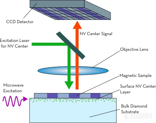
CCD与显微镜成像
2. 单个NV色心研究:样品表面的纳米金刚石
纳米金刚石的单个NV色心探测可以通过共聚焦显微技术来实现。实验装置包括三维低温纳米位移台,Z方向可以调整样品到焦平面,XY可以对样品表面进行扫描。Montana Instruments设计方案可以采用高数值孔径物镜对4K的样品中的单个NV色心进行测量。系统的收集效率高、光斑直径小,轻松聚焦单个NV色心。采用532nm激光激发,对630nm-800nm范围的荧光信号进行采集。采用可调的微波信号对NV色心的自旋态进行激发,通过荧光信号的峰值位移来确定其自旋态。为了研究感兴趣的区域,通常将金刚石粉末(20-30nm)均匀的撒在样品表面,然后使用三维纳米位移台来扫描样品并且对特定NV色心进行测量。并且可以通过单个NV色心实现在较大温度范围内对样品的性质进行观测。
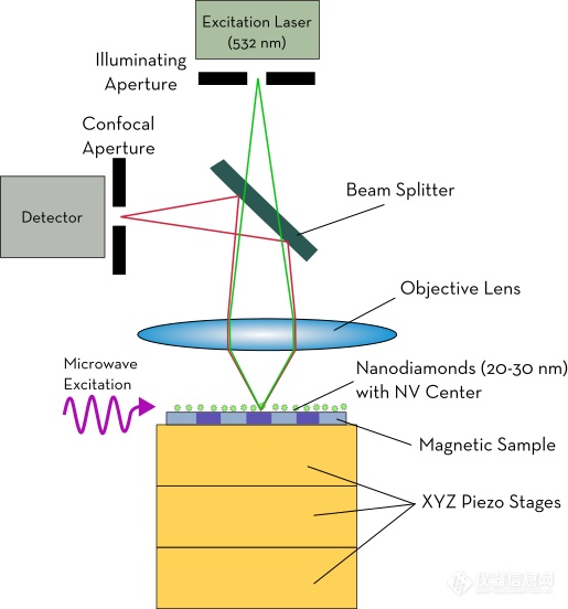
扫描共聚焦显微镜
Tokura课题组成功的运用此技术研究了FeGe样品中的磁涡旋结构。实验细节请参考:
Using NV-Center Optically Detected Magnetic Resonance (ODMR) as a Probe for Local Magnetic Dynamics in Transition Metals
3. 扫描探针量子探测器(例如,扫描磁力显微镜)
我们将一个NV色心固定在扫描探针显微镜的探针末端。可以通过在针上“粘贴”纳米金刚石,或采用纳米压印与O2刻蚀技术将块体金刚石加工成再用N-14注入来实现NV色心,现在甚至已经有商业化的针。采用共聚焦显微镜将激发光聚焦在扫描探针的NV色心上。样品可以通过低温纳米位移台进行扫描。这样便实现了对样品表面的纳米精度大范围成像测量。该技术理论上可以对多种与NV色心荧光相关的特性进行高精度显微学测量。
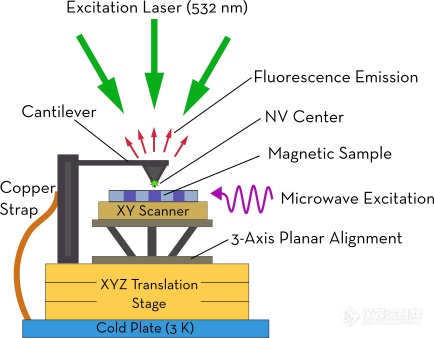
扫描探针显微镜
Jayich课题组 (UCSB)运用这一技术在BaFe2(As0.7P0.3)2 超导材料的转变温度附近(30K)成功观测到了vortices。这一技术在研究材料低温下的新奇性质方面前景广阔。更多细节请参考:
Scanned probe imaging of nanoscale magnetism at cryogenic temperatures with a single-spin quantum sensor.
■ 高性能低温恒温器在量子计算中的应用
Cryostation®低温恒温器系统可为量子计算相关研究提供多种解决方案,丰富的可选配置与配件可以满足各种实验的需求,诸如离子阱、超导环、NV色心的高数值孔径荧光观测等。根据具体实验需求Montana Instruments可以提供适合的配置方案。
量子计算实验案例:RF离子阱
配置方案:高数值孔径荧光读出、多光学通道用于激光制冷、RF+DC电学通道用于制造囚禁势阱。
作为该实验方案的核心,离子阱量子计算包括N个囚禁离子。离子可以被囚禁在泡利(RF)阱或彭宁(磁场)阱中,每个囚禁离子具有两个态或亚稳态。这里我们简单讨论泡利阱的情况,实验上泡利阱是通过在样品上印制一组具有特殊几何形状的RF电产生限制电势实现的。在设计好势阱后我们通过激光烧蚀衬底产生一个待囚禁的离子(常用137Yb+),采用多普勒或Sisyphus冷却方案用激光将高度激发状态的离子冷却至量子态。后再将离子导入精心设计的势阱中。
待离子进入势阱中,将他们在空间上隔开几微米的距离,每个离子代表一个量子比特。量子比特通过库伦相互作用影响量子比特的集体震荡来实现耦合。每一个量子比特都通过与库伦势的“平行”或“反平行”将自己的局部态编码进集体震动。这样每一个在一维链上的量子比特都实现了与其他每个量子比特的耦合。
量子计算的通用“门”操作(CROT, SWAP以及内部量子比特态的任意翻转)可以通过对量子比特光激发来实现。对于137YB+离子链,佳波长为355nm。激光源的稳定性尤为重要,激发频率与电子的共振频率要匹配(10KHz或更好),以防止其他临近态的激发。紫外激光由于具有合适的波长与佳的频率稳定性常被用于半导体材料的维纳加工,现在也成为量子计算的上佳选择。
量子比特在经过一系列量子算法的门操作后的量子态可以被读出。囚禁离子的量子态读出是通过测量与量子态相关的荧光实现的。目前的研究通常利用高数值孔径的显微镜可以实现10%左右的收集效率。未来的量子计算可能会通过集成光学微腔的方案来提高荧光光子的收集效率,预计可以大于50%。该集成技术也可以推动可拓展与重构的量子计算电路发展。
总的来说,设计和操纵一个可靠的离子阱量子计算机需要1、稳定的激光源与的频率控制。2、有效且控制良好的RF电势来定位与控制囚禁离子。3、数字控制的空间分辨率很高的脉冲激光来制备、测量、操纵量子比特。4、量子态的可靠探测与读出。
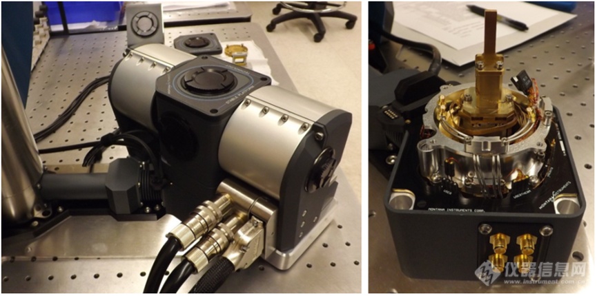
Montana Instruments与科研人员共同设计的离子阱量子计算机
MI恒温器与集成式单光子探测器有望提高离子阱的量子态读出
参考文献:
[1] ohnson, K. G. et al. Active Stabilization of Ion Trap Radiofrequency Potentials. Review of Scientific Instruments 87, 53110 (2016).
[2] Brown, K. R., Kim, J. & Monroe, C. Co-Designing a Scalable Quantum Computer with Trapped Atomic Ions. npj Quantum Information 16034 (2016).
[3] Debnath, S. et al. Demonstration of a small programmable quantum computer with atomic qubits. Nature 536, 63–66 (2016).
[4] Steane, A. M. The Ion Trap Quantum Information Processor. Applied Physics B: Lasers and Optics 64, 623–643 (1997).
[5] Faraz Najafi et al. On-chip detection of non-classical light by scalable integration of single-photon detectors.
■ 高性能低温恒温器在自旋电子学中的应用
科研中MOKE常用来表征材料的电子和磁学特征,例如磁畴结构、自旋态密度、磁相变动力学。在高质量纳米结构和2D材料中新的实验进展表明,有望在集成的光子或自旋电子器件中利用磁光效应在纳米尺度上加强对光的控制。
MOKE实验需要灵活的光路与电学通道以及磁场环境。样品需要一个超稳定的低温环境并且能够调整配置以适应实验需求的多种几何光路。Cryostation基础系统与成熟的选件库可为MOKE提供多种解决方案。通过不同的搭配组合我们可以轻松实现磁光克尔效应、光磁测量、光致发光、偏振分辨测量、自旋输运与动力学、磁畴壁移动、磁阻研究、电学和高频测量、输运性质等方面的研究。以下是部分低温磁光克尔效应实验举例:
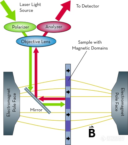
1. 纵向磁光克尔效应
在纵向MOKE的几何光路中,磁场与样品表面平行,样品中的磁畴平行于磁场方向。激光光源通过偏振器实现设定的偏振。光线通过物镜聚焦在样品感兴趣的区域上。入射光线与样品的磁畴发生相互作用使得反射光线偏振方向改变。偏振方向改变的幅度与局部磁化的强度成比例。通过仪器接收并分析反射光线的克尔转角就可以得到局部磁矩的方向和强度信息。这种测量方案所需的样品环境可以在集成了双性电磁铁的低温恒温器中来实现,例如Cryostation与Magneto-Optic。
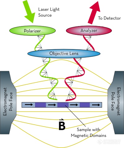
利用纵向克尔效应的宏观磁畴图像测量方案
2. 极向磁光克尔效应
在向克尔几何光路中,磁场沿样品表面的发现方向(适用于面外易磁化轴样品)。此时磁化方向垂直于样品表面,为了大化的收集信号,入射激光需要垂直照射在样品表面。与纵向克尔类似,入射激光的偏振方向在被磁性样品表面反射时会发生轻微的偏转。偏转的程度与局部磁畴的强度和方向有关。在Cryostation与Magneto-Optic装置中,与纵向克尔相比,样品旋转了90°,并且在磁中间引入了一个小的反射镜来实现入射光线与磁场的平行以及与样品表面的垂直。
极向MOKE宏观磁畴测量方案
3. 时间分辨MOKE
可以用时间分辨(瞬态)的MOKE对脉冲磁场和脉冲电场驱动的磁畴壁移动进行动力学研究。举例来说,可以对用于磁带存储器研究的磁性纳米线中的磁畴壁移动进行测量。磁畴壁通常在预定的位置有电脉冲或磁脉冲注入纳米线。利用MOKE信号对纳米线的局部进行探测,空间分辨率可优于1um,时间分辨率可达到150fs。如果t=0时刻对应于畴壁注入,对指定区域沿纳米线进行延时脉冲扫描观察MOKE信号的变化。MOKE信号的变化对应磁畴壁移动所引起的磁性翻转。通过测量纳米线不同位置MOKE信号的变化时间可以计算出畴壁的移动速度。
时间分辨MOKE也可以用于研究自旋“群体”的寿命。利用化的泵浦光对感兴趣的材料进行自旋激发。利用探测光进行延时扫描,MOKE信号的强弱可以计算自旋“群体”密度。自旋的“寿命”可以通过观测自旋“群体”的密度来计算。Kawakami课题组(Ohio State University)利用该方法对过渡族金属二硫化物WS2在低温(<6K)下进行了时间分辨克尔转角测量(TRKR)。对比TRKR信号与显微荧光,研究者发现强激子发光与高自旋密度之间的一种意料之外的反相关关系。这一发现为短时激子自旋角动量到长时导电电子自旋态转化提供了新的见解。
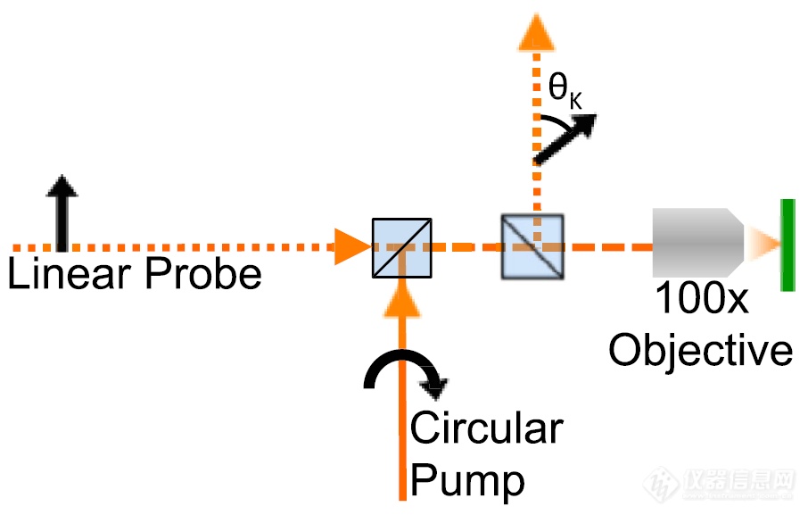
时间分辨克尔效应的原理与装置图
4. 强磁场(>1T)MOKE
华盛顿大学的Xu和Cobden 利用7T的超导磁体与低温设备,采用法拉几何光路测量磁场对光致发光化的影响对单层WSe2进行了研究。更多信息请阅读:Magnetic Control of Valley Pseudospin: A Story of Symmetry.
参考文献:
[1] Durham Magneto Optics Ltd & Beguivin, A. Characterization of the Montana Instruments Cryostation C2 for low temperature Magneto-Optical Kerr Effect measurements using the NanoMOKE 3.
[2] Bushong, E. J. et al. Imaging Spin Dynamics in Monolayer WS2 by Time-Resolved Kerr Rotation Microscopy. arXiv:1602.03568 [cond-mat] (2016).
[3] Aivazian, G. et al. Magnetic Control of Valley Pseudospin in Monolayer WSe2. Nature Physics 11, 148–152 (2015).
[4] Henn, T. et al. Ultrafast supercontinuum fiber-laser based pump-probe scanning MOKE microscope for the investigation of electron spin dynamics in semiconductors at cryogenic temperatures with picosecond time and micrometer spatial resolution. Review of Scientific Instruments 84, 123903 (2013).
发表文章
Montana Cryostation 用户发表文章选集(2012-2020)。分类仅供参考,可能存在偏差,文章学术价值与排序无关。
■ 二维材料、激子
Nature Physics; Excitonic Luminescent Up-Conversion in a 2D Semiconductor
Nature Physics; Spin–phonon interactions in silicon carbide addressed by Gaussian acoustics
Nature Nanotechnology; Probing dark excitons in atomically thin semiconductors via near-field coupling to surface plasmon polaritons
Nature Nanotechnology; Electrical control of charged carriers and excitons in atomically thin materials
Nature Communications; Cascaded emission of single photons from the biexciton in monolayered WSe2
Nano Letters; Quantifying remote heating from propagating surface plasmon polaritons
Nano Letters; Giant Enhancement of Defect-Bound Exciton Luminescence and Suppression of Band-Edge Luminescence in Monolayer WSe2–Ag Plasmonic Hybrid Structures
Physical Review Letters; Large Excitonic Reflectivity of Monolayer MoSe2 Encapsulated in Hexagonal Boron Nitride.
ACS Nano; Photoluminescent Quantum Interference in a van der Waals Magnet Preserved by Symmetry Breaking
ACS Photonics; Strain-Correlated Localized Exciton Energy in Atomically Thin Semiconductors
Physical Review B; Role of strain on the coherent properties of GaAs excitons and biexcitons
Physical Review B; Signatures of four-particle correlations associated with exciton-carrier interactions in coherent spectroscopy on bulk GaAs
Physical Review Materials; Laser Annealing for Radiatively Broadened MoSe2 grown by Chemical Vapor Deposition
Science Advances; Persistent Optical Gating of a Topological Insulator
Science Advances; Optical generation of high carrier densities in 2D semiconductor heterobilayers
■ 范德瓦耳斯异质结
Nature Communications; Observation of Long-Lived Interlayer Excitons in Monolayer MoSe2-WSe2 Heterostructures
Nano Letters; Single Defect Light-Emitting Diode in a van der Waals Heterostructure
Nano Letters; Interlayer Exciton Optoelectronics in a 2D Heterostructure p-n junction
Nano Letters; Nanocavity Integrated van der Waals Heterostructure Light-Emitting Tunneling Diode
Nano Letters; Unusual Exciton-Phonon Interactions at van der Waals Engineered Interfaces
Physical Review Letters; Controlling excitons in an atomically thin membrane with a mirror
■ 自旋谷
Science; Valley-Polarized Exciton Dynamics in a 2D Semiconductor Heterostructure
Nature Physics; Magnetic Control of Valley Pseudospin in Monolayer WSe2
Nature Communications; Directional Interlayer Spin-Valley Transfer in 2D Heterostructures
Nature Communications; Coulomb-bound four- and five-particle valleytronic states in an atomically-thin semiconductor.
Science Advances; Observation of ultralong valley lifetime in WSe2/MoS2heterostructures
■ 石墨烯
Nature; Proton-assisted growth of ultra-flat graphene films
Nature Physics; Photo-Nernst Current in Graphene
ACS Nano; Lithographically Patterned Functional Polymer–Graphene Hybrids for Nanoscale Electronics
Applied Physics Letters; Direct and parametric synchronization of a graphene self-oscillator
■ 光力研究
Nature Communications; Nonlinear cavity optomechanics with nanomechanical thermal fluctuations
Science; Quantum correlations from a room-temperature optomechanical cavity
Physical Review X; Single-Crystal Diamond Nanobeam Waveguide Optomechanics
Physical Review Letters; Optomechanical Quantum Control of a Nitrogen-Vacancy Center in Diamond
■ 超导材料相关测量
Scientific Reports; Imprinting superconducting vortex footsteps in a magnetic layer
Scientific Reports; Triode for Magnetic Flux Quanta
Physical Review B; Magnetic flux penetration in Nb superconducting films with lithographically defined micro-indentations
Physical Review B; Impurity scattering effects on the superconducting properties and the tetragonal-to-orthorhombic phase transition in FeSe
Physical Review B; Crossing fields in thin films of isotropic superconductors
Physical Review B; Flux penetration in a superconducting film partially capped with a conducting layer
■ 电荷密度波
Nature Nanotechnology; Strongly enhanced charge-density-wave order in monolayer NbSe2
Nature Communications; Patterns and driving forces of dimensionality-dependent chargedensity waves in 2H-type transition metal dichalcogenides
Arxiv; Two Phonon Interactions and Charge Density Wavein Single Crystalline VSe2 Probed by Raman Spectroscopy
■ 磁学测量相关
Nature; Layer-dependent ferromagnetism in a van der Waals crystal down to the monolayer limit
Nature; Three-state nematicity in the triangular lattice antiferromagnet Fe1/3NbS2
Science;Measuring magnetic field texture in correlated electron systems under extreme conditions
Nature Physics; Ligand-field helical luminescence in a 2D ferromagnetic insulator
Nature Nanotechnology; Scanned probe imaging of nanoscale magnetism at cryogenic temperatures with a single-spin quantum sensor
Nature Nanotechnology; Electrical control of 2D magnetism in bilayer CrI3
Nature Communications; Local dynamics of topological magnetic defects in the itinerant helimagnet FeGe
Nature Communications; Spin transfer torque driven higher-order propagating spin waves in nano-contact magnetic tunnel junctions
PNAS; Local optical control of ferromagnetism and chemical potential in a topological insulator
Scientific Reports; Spin noise explores local magnetic fields in a semiconductor
2D Materials; Imaging Spin Dynamics in Monolayer WS2 by Time-Resolved Kerr Rotation Microscopy
Physical Review B; Upper critical fields in Ba2Ti2Fe2As4O single crystals: Evidence for dominant Pauli paramagnetic effect
Journal of Applied Physics; Thickness- and temperature-dependent magnetodynamic properties of yttrium iron garnet thin films
IOP Superconductor Science and Technology; Transport characterization and pinning analysis of BaFe1.9Ni0.1As2.05 thin films
Review of Scientific Instruments; Scanning SQUID microscopy in a cryogen-free cooler
■ 量子存储
Nature Communications; Storage of multiple single-photon pulses emitted from a quantum dot in a solid-state quantum memory
Physical Review X; A 10-qubit solid-state spin register with quantum memory up to one minute
Physical Review Letters; Coherent spin control at the quantum level in an ensemble-based optical memory
Physical Review Letters: Solid state source of non-classical photon pairs with embedded multimode quantum memory
Physical Review A; A spectral hole memory for light at the single photon level
Physical Review A; Towards highly multimode optical quantum memory for quantum repeaters
New Journal of Physics; Storage of up-converted telecom photons in a doped crystal
New Journal of Physics; Cavity-enhanced storage in an optical spin-wave memory
New Journal of Physics; Multiplexed on-demand storage of polarization qubits in a crystal
AIP Conference Proceedings; Realization of the revival of silenced echo (ROSE) quantum memory scheme in orthogonal geometry
■ 量子点散射
Nature Photonics; All-optical coherent control of vacuum Rabi oscillations
Nature Communications; Nanoscale optical positioning of single quantum dots for bright and pure single-photon emission
Physical Review Letters; Field-Field and Photon-Photon Correlations of Light Scattered by Two Remote Two-Level InAs Quantum Dots on the Same Substrate
Physical Review B; Coherent versus Incoherent Light Scattering from a Quantum Dot
Physical Review B; Bichromatic Resonant Light Scattering from a Quantum Dot
Physical Review B; Two-Color Photon Correlations of the Light Scattered by a Quantum Dot
Physical Review A; Resonant light scattering of a laser frequency comb by a quantum dot
Advanced Optical Materials; Localized all-optical control of single semiconductor quantum dots through plasmon-polariton-induced screening
■ 量子阱
Applied Physics Letters; Highly polarized photoluminescence and its dynamics in semipolar (2021) InGaN/GaN quantum well
Applied Physics Letters; Impact of carrier localization on radiative recombination times in semipolar plane (2021)InGaN/GaN quantum wells
Physica Status Solidi C; Optical properties and carrier dynamics in m-plane InGaN quantum wells
Optical Materials Express; Influence of well width fluctuations on recombination properties in semipolar InGaN quantum wells studied by time- and spatially-resolved near-field photoluminescence
■ 量子信息、量子计算等
Nature; Photonic quantum state transfer between a cold atomic gas and a crystal
Nature; Deterministic delivery of remote entanglement on a quantum network
Science; Probing Johnson noise and ballistic transport in normal metals with a single-spin qubit
Science; Entanglement Distillation between Solid-State Quantum Network Nodes
Nature Physics; Accelerated quantum control using superadiabatic dynamics in a solid-state lambda system
Nature Communications; Coherent Acoustic Control of a Single Silicon Vacancy Spin in Diamond
Physical Review Letters; Multimode and Long-Lived Quantum Correlations Between Photons and Spins in a Crystal
Optics Express; Two-pulse photon echo area theorem in an optically dense medium
AIP Conference Proceedings; Photon echo area theorem for Gaussian laser beams
IEEE Xplore; Towards Millimeter-Wave Based Quantum Networks
■ 基础量子力学研究
Nature; Loophole-free Bell inequality violation using electron spins separated by 1.3 kilometres
Scientific Reports; Loophole-free Bell test using electron spins in diamond: second experiment and additional analysis
■ 金刚石
Nature Communications; Coherent control of a strongly driven silicon vacancy optical transition in diamond
Physical Review X; Coupling a Surface Acoustic Wave to an Electron Spin in Diamond via a Dark State
Physical Review Letters; Protecting a Solid-State Spin from Decoherence Using Dressed Spin States
Physical Review Letters; Opticallly-driven Rabi oscillations and adiabatic passage of single electron spins in diamond
Physical Review Letters; Holonomic quantum control by coherent optical excitation in diamond
Physical Review A; Strain coupling of a mechanical resonator to a single quantum emitter in diamond
CLEO; Lead-Related Quantum Emitters in Diamond
Journal of Carbon Research; Fluorescence and Physico-Chemical Properties of Hydrogenated Detonation Nanodiamonds
■ 金刚石色心、量子点荧光、单光子发射等
Nature Photonics; 4H-silicon-carbide-on-insulator for integrated quantum and nonlinear photonics
Nature Communications; Optical charge state control of spin defects in 4H-SiC
Nature Communications; Extremely rapid isotropic irradiation of nanoparticles with ions generated in situ by a nuclear reaction
Nature Communications; Bright room temperature single photon source at telecom range in cubic silicon carbide
Nature Communications; Spin-controlled generation of indistinguishable and distinguishable photons from silicon vacancy centres in silicon carbide
Physical Review X; Quantum Interference of Electromechanically Stabilized Emitters in Nanophotonic Devices
Physical Review Letters; Polarization-Dependent Interference of Coherent Scattering from Orthogonal Dipole Moments of a Resonantly Excited Quantum Dot
Optics Express; Optical coherence of implanted silicon vacancy centers in thin diamond membranes
Scientific Reports; Single-photon property characterization of 1.3?μm emissions from InAs/GaAs quantum dots using silicon avalanche photodiodes
Scientific Reports; Combined atomic force microscopy and photoluminescence imaging to select single InAs/GaAs quantum dots for quantum photonic devices
Physical Review B; Characterization of 171Yb3+: YVO4 for photonic quantum technologies
Physical Review B; Characterization of optical and spin properties of single tin-vacancy centers in diamond nanopillars
Optica; Two-photon interference from a bright single-photon source at telecom wavelengths
Optica; Efficient fiber-coupled single-photon source based on quantum dots in a photonic-crystal waveguide
Photonics; Scalable fabrication of single silicon vacancy defect arrays in silicon carbide using focused ion beam
ACS Nano; Self-Assembled Nanocrystals of Polycyclic Aromatic Hydrocarbons Show Photostable Single-Photon Emission
ACS Photonics; Towards bright and pure single photon emitters at 300 K based on GaN quantumdots on silicon
CLEO; Characterization of the Local Charge Environment of a Single Quantum Dot via Resonance Fluorescence
Journal of Applied Physics; Photoexcited carrier trapping and recombination at Fe centers in GaN
Physical Review Applied; Single Self-Assembled InAs / GaAs Quantum Dots in Photonic Nanostructures: The Role of Nanofabrication
■ 微腔相关研究
Nature Photonics; Quantum control of a spin qubit coupled to a photonic crystal cavity
Nature Communications; All-optical polariton transistor
Nature Communications; Spin–cavity interactions between a quantum dot molecule and a photonic crystal cavity
Nature Communications; Interaction-induced hopping phase in driven-dissipative coupled photonic microcavities
Nature Communications; Interfacing broadband photonic qubits to on-chip cavity-protected rare-earth ensembles
Nano Letters; Strongly Cavity-Enhanced Spontaneous Emission from Silicon-Vacancy Centers in Diamond
Physical Review Letters; Bosonic Condensation and Disorder-Induced Localization in a Flat Band
Physical Review Letters; Ultrastable Silicon Cavity in a Continuously Operating Closed-Cycle Cryostat at 4 K
Physical Review Letters; Probing a Dissipative Phase Transition via Dynamical Optical Hysteresis
Physical Review Letters; Cavity-enhanced Raman emission from a single color center in a solid
Optics Express; A High-Mechanical Bandwidth Fabry-Perot Fiber Cavity
Physical Review B; Multidimensional coherent spectroscopy of a semiconductor microcavity
Physical Review Applied; Engineering Phonon Leakage in Nanomechanical Resonators
Applied Physics Letters; Controlled coupling of photonic crystal cavities using photochromic tuning
Applied Physics Letters; Design and low-temperature characterization of a tunable microcavity for diamond-based quantum networks
■ 纳米结构、光子晶体、异质结
Physical Review Letters; Franson Interference Generated by a Two-Level System
Nano Letters; Electrically Driven Hot-Carrier Generation and Above-threshold Light Emission in Plasmonic Tunnel Junctions
ACS Photonics; Monolithic High-Contrast Grating Based Polariton Laser
ACS Photonics; Epitaxial Aluminum-on-Sapphire Films as a Plasmonic Material Platform for Ultraviolet and Full Visible Spectral Regions
CLEO; Diamond Optomechanical Crystals at Cryogenic Temperatures
Laser Physics Letters; Observation and investigation of narrow optical transitions of 167Er3+ ions in femtosecond laser printed waveguides in 7LiYF4 crystal
IOP Science Applied Physics Express; Single-step direct laser writing of halide perovskite microlasers
Rapid Research Letters; Radiative Efficiency and Charge-Carrier Lifetimes and Diffusion Length in Polycrystalline CdSeTe Heterostructures
■ 发光材料
Nature Communications; Electronic Raman scattering as an ultra-sensitive probe of strain effects in semiconductors
Applied Physics Letters; High quality factor single-crystal diamond mechanical resonators
New Journal of Physics; Shifts of optical frequency references based on spectral-hole burning in Eu3+:Y2SiO5
Journal of Luminescence; Evaluation of defects in cuprous oxide through exciton luminescence imaging
SPIE; Tailoring of GaAs/GaAsSb core-shell structured nanowires for IR photodetector applications
2D Materials; Magneto-Elastic Coupling in a potential ferromagnetic 2D Atomic Crystal
■ 穆斯堡尔谱
Carbon Letters; One-step microwave synthesis of magnetic biochars with sorption properties
Inorganic Chemistry; Screw-Type Motion and Its Impact on Cooperativity in BaNa2Fe[VO4]2
■ 光伏、热电、储能材料
Nano Letters; Photothermoelectric Detection of Gold Oxide Nonthermal Decomposition
Scientific Reports; Optically induced metastability in Cu(In,Ga)Se2
ACS Nano; Plasmonic heating in Au nanowires at low temperatures: The role of thermal boundary resistance
ACS Nano; Room-Temperature Electrocaloric Effect in Layered Ferroelectric CuInP2S6 for Solid-State Refrigeration
Physical Review B; Thermally Driven Long Range Magnon Spin Currents in Yttrium Iron Garnet due to Intrinsic Spin Seebeck Effect
Applied Physics Letters; The impact of Cu on recombination in high voltage CdTe solar cells
Applied Physics Letters; Local Phonon Mode in thermoelectric Bi2Te2Se from charge neutral antisites
Journal of Physical Chemisty Letters; Photothermoelectric effects and large photovoltages in plasmonic Au nanowires with nanogaps
Energy Procedia; Low-temperature FTIR investigation of aluminum doped solargrade silicon
IEEE Journal of Photovoltaics; Minority-Carrier Lifetime and Surface Recombination Velocity in Single-Crystal CdTe
Nanoscale; Substantial local variation of Seebeck coefficient in gold nanowires
SPIE Digital Library; Photovoltages and hot electrons in plasmonic nanogaps
International Journal of Heat and Mass Transfer; Grain growth-induced thermal property enhancement of NiTi shape memory alloys for elastocaloric refrigeration and thermal energy storage systems
■ 新型钙钛矿材料
Physical Review Materials; Stable biexcitons in two-dimensional metal-halide perovskites with strong dynamic lattice disorder
ACS Chemistry of Materials; Electron–Phonon Couplings Inherent in Polarons Drive Exciton Dynamics in Two-Dimensional Metal-Halide Perovskites
ACS Journal of Physical Chemistry C; Photoluminescence Manipulation by Ion Beam Irradiation in CsPbBr3 Halide Perovskite Single Crystals
Advanced Optical Materials; Amplified Spontaneous Emissionand Random Lasing in MAPbBr3 Halide Perovskite Single Crystals
Arxiv; Defect-related states in MAPbI3halide perovskite single crystals revealed by the photoluminescence excitation spectroscopy
■ 纳米线
Physical Review Letters; Widely Tunable Single-Photon Source from a Carbon Nanotube in the Purcell Regime
Semiconductor Science and Technology; Bandgap tuning of GaAs/GaAsSb core-shell nanowires grown by molecular beam epitaxy
IOP Nanotechnology; Space charge limited conduction mechanism in GaAsSb nanowires and the effect of in-situ annealing in ultra-high vacuum
■ 生物、有机分子
Journal of Physical Chemistry Letters; Increased Transfer Efficiency from Molecular Photonic Wires on Solid Substrates and Cryogenic Conditions
ACS Applied Nano Materials; DNA Origami Chromophore Scaffold Exploiting HomoFRET Energy Transport to Create Molecular Photonic Wires
Physical Review A;Quantum dynamics of a driven two-level molecule with variable dephasing
■ 其他研究方向
AIP Conference Proceedings; The equipment control system of the extended x-ray absorption fine structure beamline at Taiwan Photon Source
ACS Applied Nano Materials.; Elimination of Extreme Boundary Scattering via Polymer Thermal Bridging in Silica Nanoparticle Packings: Implications for Thermal Management
Arxiv; Observation of three-state nematicity in the triangular lattice antiferromagnet Fe1/3 NbS2
Arxiv; Ferroelectric Polarization in Antiferroelectric Chalcogenide Perovskite BaZrS3 Thin Fil
用户单位
采购时间
采购数量
中科院半导体所
2013/02/14
1
中科院物理所
2013/02/15
2
中国科技大学
2013/03/13
2
中国科学技术大学
2012/02/29
1
苏州纳米所
2012/02/29
1
首都师范大学
2011/09/28
1
山西大学
2011/07/11
1
Montana Instrument低温恒温器CryoAdvance系列的工作原理介绍
低温恒温器CryoAdvance系列的使用方法?
Montana InstrumentCryoAdvance系列多少钱一台?
低温恒温器CryoAdvance系列可以检测什么?
低温恒温器CryoAdvance系列使用的注意事项?
Montana InstrumentCryoAdvance系列的说明书有吗?
Montana Instrument低温恒温器CryoAdvance系列的操作规程有吗?
Montana Instrument低温恒温器CryoAdvance系列报价含票含运吗?
Montana InstrumentCryoAdvance系列有现货吗?
更多![]()

更多![]()

高质量石墨烯制备及拉曼表征
南京大学高力波教授、奚啸翔教授等多个课题组合作,采用质子辅助的CVD方法生长制备出了无褶皱的超平石墨烯。该方法成功解决了传统CVD制备石墨烯过程中由于石墨烯与基质材料强耦合作用而形成的褶皱,这为石墨烯在二维电子器件等领域的应用扫除了一大障碍。文章表明,在质子辅助的CVD制备方法中,质子能够渗透石墨烯,对石墨烯和衬底之间的范德瓦尔斯相互作用进行去耦合,使褶皱完全消失。该方法还可以对传统CVD制备过程中产生的褶皱进行很大程度的去除。此外,通过新方法制备的超平石墨烯材料,不仅具有优异的清洁能力,还在测量中展示了室温量子霍尔效应。研究认为,质子辅助的CVD方法不仅能制备出高质量的石墨烯,并且对制备其他种类的纳米材料具有普适性,为制备高质量的二维材料提供了一种新途径。相关成果发表在Nature。 值得一提的是,文章中对样品进行了高质量的变温Raman测量(Montana Instruments公司生产的Cryostation®系列高性能恒温器与普林斯顿光谱仪联合测量完成),清晰的展示了不同制备与处理条件的石墨烯G峰和2D峰随温度变化的峰位移动。揭示了石墨烯与衬底之间相互作用的强弱以及石墨烯受到的应力大小。
材料
2020/04/07
企业名称
QUANTUM量子科学仪器贸易(北京)有限公司
企业信息已认证
企业类型
信用代码
110000410217679
成立日期
2004-10-10
注册资本
20
经营范围
磁性物体测量系统、物理性物体测量系统、超导量子干涉装置的探头以及有关电子产品的批发、佣金代理(拍卖除外)、进出口及售后服务、咨询服务(涉及配额许可证管理、专项管理规定的商品按照国家有关规定办理)。(非货币出资4万美元。依法须经批准的项目,经相关部门批准后依批准的内容开展经营活动。)
QUANTUM量子科学仪器贸易(北京)有限公司
公司地址
北京市朝阳区酒仙桥路10号恒通商务园B22座 501 室
客服电话
公司名称: QUANTUM量子科学仪器贸易(北京)有限公司
公司地址: 北京市朝阳区酒仙桥路10号恒通商务园B22座 501 室 联系人: 市场部 邮编: 100015 联系电话: 400-860-5168转0980
仪器信息网APP

展位手机站